|
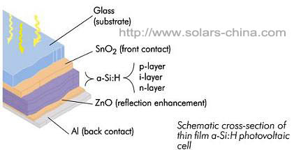
Amorphous silicon (a-Si) is the non-crystalline form of silicon. The material can be alloyed with hydrogen to form hydrogenated amorphous silicon (a-Si:H) resulting in a significantly lower number of defects and hence a practical material for semi-conductive device applications, including photovoltaic. Amorphous silicon pv solar modules are made with thin layers of a-Si:H on a conductive substrate. Amorphous silicon-based thin-film pv solar modules were invented in 1976, and have since been successfully used in a wide range of solar battery applications for several decades. Here is a typical module structure:

There are several key advantages to a-Si:H based thin-film PV modules. First, a-Si thin-film can be deposited onto a variety of substrates at relatively low temperatures, presenting many interesting application opportunities. Second, a-Si thin film can be deposited over large areas by PECVD (plasma enhanced chemical vapor deposition) technology. Third, a-Si thin film modules use silicon, which is abundant and environmental friendly, as compared to the materials needed for other thin film technologies.
|
Thin-film based PV modules offer a great opportunity to reduce manufacturing costs. One reason is that very little material is needed for each module. The energy consumed in the thin film PV manufacturing process is significantly less than that consumed in the crystalline silicon PV module manufacturing process. In addition, thin film PV modules are significantly thinner than conventional crystalline solar PV modules. As a result, the silicon materials used in thin film PV module manufacturing are only approximately 1% to 2% of those used to produce crystalline silicon PV modules. Another is that thin-film cells can be constructed monolithically, lending to great degree of process automation. |

Amorphous silicon-based technologies have improved significantly over the past 30 years. Advances have been made in several aspects of a-Si technology:
Cell Structure Optimization
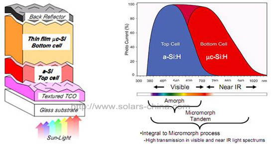
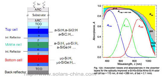
In multiple-junction design, stacks of cells sensitive to different portion of the solar spectrum combine to significantly increase the conversion efficiency. Designs involving silicon-germanium alloy (a-Si/a-SiGe:H) or micro-crystalline (a-Si/µc-Si :H), have been successfully commercialized.
Illustration of an a-Si/µc-Si tandem cell:

Example of a triple junction cell:

Recent research and development has focused on innovative optical designs of the front and back transparent conductive oxides, such as Internal Light Trapping techniques, to enhance cell conversion efficiency and reduce the effect of light-induced degradation.
Deposition Technology
PECVD technology has undergone great improvement, in areas such as very high frequency power source and vapor chamber design, resulting in increased deposition rates and higher layer quality.
Materials
There have been extensive research and development efforts in the uses of various silanes and gas mixture with the objectives of improving deposition efficiency and achieving desirable layer properties.
Module Construction
To offer low cost of power generation by PV technology, the power modules must have a long operating life, e.g. over 30 years. Key to this longevity is the protective encapsulation technology that insulates the cells from the harmful effects of moisture and oxygen. Various high performance polymeric encapsulation materials have been introduced into a-Si module construction.
View PDF:  Amorphous thin film technology Amorphous thin film technology
More solar product,please visit our webwist: http://www.solars-china.net
|